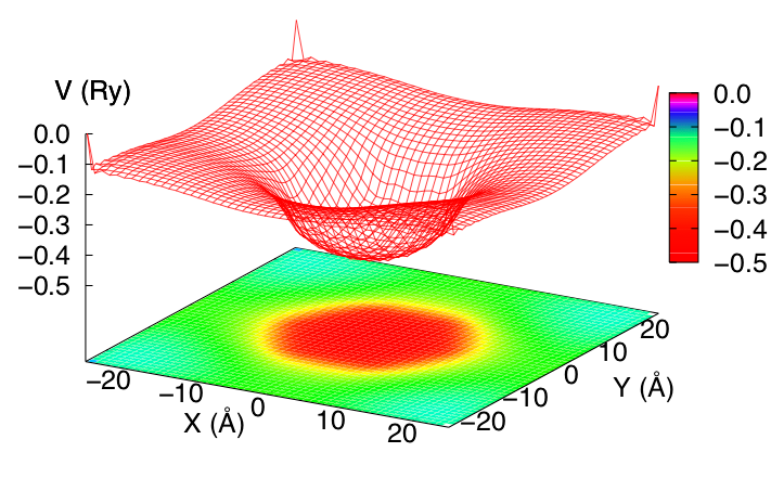
An important source of scattering for charge carriers is the presence of impurities, which are both undesired defects, by-products of an imperfect growth, and dopants, which are purposely introduced to provide the material with tailor-made electric features. Clearly, this case is the most challenging: dopants increase the carrier density at device operation temperature, but at the same time might induce a significant scattering, which leads to a drop in the conductance. With the reduction of the wire size, the impurity cross sections can become of the same order of the wire characteristic dimension and can result in total backscattering. In the semiclassical picture used to study transport in bulk materials, impurities are pointlike centers that scatter randomly the incoming carriers. This chaotic process slows down the carrier flow and results in a reduction of the conductance. The quantum picture in a thin one-dimensional medium is slightly different: impurities have to go through to a scattering potential that often extends throughout most of the wire cross section and, following with the semiclassical analogy, the trajectories of the carriers are not simply deviated, but they can be entirely backscattered.
Selected publications
R. Rurali and N. Lorente, Metallic and semimetallic <100> silicon nanowires, Phys. Rev. Lett. 94, 026805 (2005)
T. Markussen, R. Rurali, A.-P. Jauho, and M. Brandbyge, Scaling theory put into practice: First-principles modeling of transport in doped silicon nanowires, Phys. Rev. Lett. 99, 076803 (2007)
R. Rurali, T. Markussen, J. Suñé, M. Brandbyge, and A.-P. Jauho, Modeling transport in ultrathin Si nanowires: Charged versus neutral impurities, Nano Lett. 8, 2825 (2008)
M. Amato, S. Ossicini, and R. Rurali, Electron Transport in SiGe Alloy Nanowires in the Ballistic Regime from First-Principles, Nano Lett. 12, 2717 (2012)
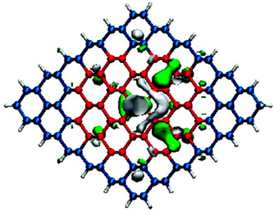
Semiconductors are privileged materials for electronics applications because their resistivities can be varied by design with much control by means of impurity doping. Equally important, they can be designed to conduct one of two types of carriers: electrons and holes. These two features are the core of device design, which relies on the interaction of adjacent semiconductors with different densities of electrons and holes. There are at least two reasons that make the physics of impurities in nanowires different with respect to bulk systems: (1) the lattice sites are no longer equivalent in the radial direction and (2) in the quantum and dielectric confinement regime doping levels are deeper with important consequences on the dopant activation. Besides impurity doping in pristine Si NWs, core-shell Si-Ge NWs and in the newly synthesized 2H-Si polytype NWs we have also centered our attention on molecular doping.
Selected publications
R. Rurali and X. Cartoixà, Theory of Defects in One-Dimensional Systems: Application to Al-Catalyzed Si Nanowires, Nano Lett. 9, 975 (2009
)
Á. Miranda-Durán, X. Cartoixà, M. Cruz Irisson, and R. Rurali, Molecular Doping and Subsurface Dopant Reactivation in Si Nanowires, Nano Lett. 10, 3590 (2010)
M. Amato, S. Ossicini, and R. Rurali, Band-Offset Driven Efficiency of the Doping of SiGe Core-Shell Nanowires, Nano Lett. 11, 594 (2011)
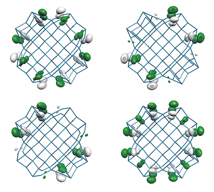
M. Amato, S. Ossicini, E. Canadell, and R. Rurali, Preferential Positioning, Stability, and Segregation of Dopants in Hexagonal Si Nanowires, Nano Lett. 19, 866 (2019)
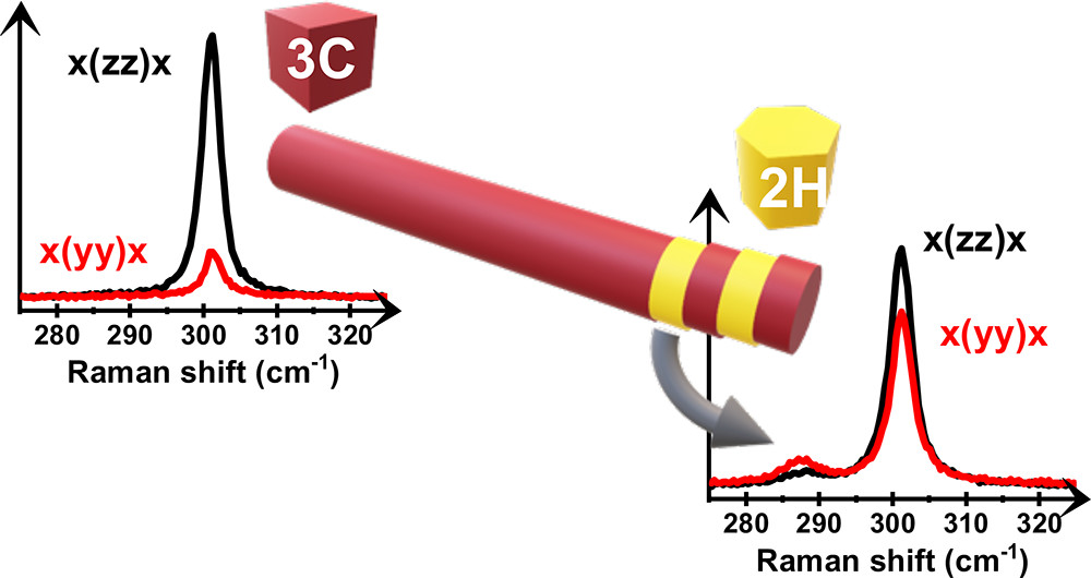
Crystal structure and interface engineering are acquiring an increasing importance in nanoscience because of their enormous potential to conceive new properties and functionalities. In the case of nanowires, the emergence of new stable polytypes of common semiconductors promises to have an important impact in materials design. The high degree of control of the growth parameters that favors one polytype over another allows creating homojunctions that are the basis for crystal phase superlattices (CPSL), a novel type of superlattice where different crystal phases of the same material, rather than different materials, are alternated with a given periodicity. These homojunctions are very special interfaces: (i) they are atomically sharp, (ii) they are defect-free, (iii) the lattice mismatch is very small, and (iv) they cannot feature any chemical intermixing. Therefore, there is a fundamental interest in the properties of these novel interfaces, particularly concerning the role they play in transport phenomena. We are lucky enough to have a fruitful collaboration on these (and other) topics with the nanophononics group led by Ilaria Zardo at the University of Basel.
Selected publications
M. Amato, T. Kaewmaraya, A. Zobelli, M. Palummo, and R. Rurali, Crystal Phase Effects in Si Nanowire Polytypes and Their Homojunctions, Nano Lett. 16, 5694 (2016)
X. Cartoixà, M. Palummo, H. I. T. Hauge, E. P. A. M. Bakkers, and R. Rurali, Optical Emission in Hexagonal SiGe Nanowires, Nano Lett. 17, 4753 (2017)
C. Fasolato, M. De Luca, D. Djomani, L. Vincent, C. Renard, G. Di Iorio, V. Paillard, M. Amato, R. Rurali, and I. Zardo, Crystalline, Phononic, and Electronic Properties of Heterostructured Polytypic Ge Nanowires by Raman Spectroscopy, Nano Lett. 18, 7075 (2018)
M. Amato, S. Ossicini, E. Canadell, and R. Rurali, Preferential Positioning, Stability, and Segregation of Dopants in Hexagonal Si Nanowires, Nano Lett. 19, 866 (2019)
Review Papers
R. Rurali, Colloquium: Structural, electronic, and transport properties of silicon nanowires, Rev. Mod. Phys. 82, 427 (2010)
M. Amato, M. Palummo, R. Rurali, and S. Ossicini, Silicon–Germanium Nanowires: Chemistry and Physics in Play, from Basic Principles to Advanced Applications, Chem. Rev. 114, 1371 (2014)
M. Amato and R. Rurali, Surface physics of semiconducting nanowires, Prog. Surf. Sci. 91, 1 (2016)
M. Royo, M. De Luca, R. Rurali, and I. Zardo, A review on III–V core–multishell nanowires: growth, properties, and applications, J. Phys. D: Appl. Phys. 50, 143001 (2017)